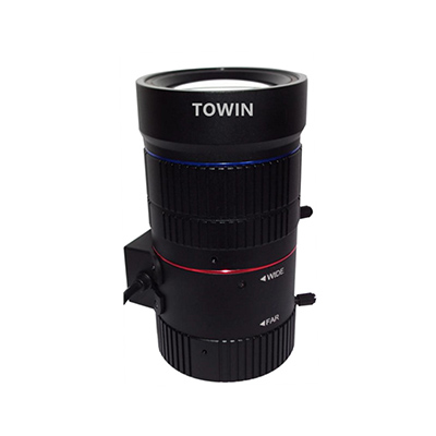
What is a zoom machine vision lens?
09/02/2025How to Clean a Fisheye Lens
09/02/2025
In the realm of optics, few components are as deceptively simple yet technically demanding as pinhole lenses. These tiny apertures, often no wider than a human hair, play a pivotal role in applications ranging from medical imaging to aerospace technology. The process of Pinhole Lens Manufacturing demands unparalleled precision, innovative engineering, and a deep understanding of material science. As industries push for smaller, more efficient, and higher-performing optical systems, manufacturers are adopting revolutionary techniques to stay ahead.
1. The Fundamentals of Pinhole Lens Manufacturing
At its core, a pinhole lens is a minute opening designed to focus light without traditional lenses. Its simplicity belies the complexity of its production. The manufacturing process involves creating a perfectly round, ultra-precise aperture in a substrate such as metal, glass, or polymer. The challenge lies in achieving sub-micron tolerances while ensuring the aperture’s edges are flawlessly smooth to minimize diffraction—a phenomenon that can degrade image quality.
2. Laser Ablation: The Gold Standard in Precision
Laser ablation has become a cornerstone of modern Pinhole Lens Manufacturing. This technique uses a focused laser beam to vaporize material, creating a clean, well-defined aperture. The key advantage? Lasers can achieve tolerances as tight as ±0.1 microns, far surpassing traditional methods. Additionally, laser ablation is non-contact, reducing the risk of mechanical stress or contamination.
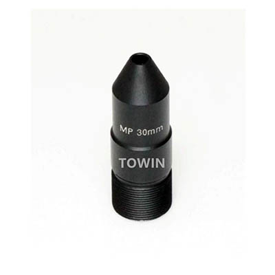
Pinhole-lens-30mm-IR-corrected-CCTV-M12-telecentric-lens
3. Ion Beam Milling: Sculpting at the Atomic Level
For applications demanding atomic-level precision, ion beam milling (IBM) stands out. This technique directs a beam of charged ions at the substrate, gradually eroding material to form the pinhole. Unlike lasers, IBM allows for ultra-smooth edges, minimizing diffraction and maximizing light throughput.
4. Photolithography: Mass Production Meets Microscale Accuracy
When volume is critical, photolithography emerges as the method of choice. Originally developed for semiconductor fabrication, this process uses light-sensitive resists to pattern substrates before etching or plating. In Pinhole Lens Manufacturing, photolithography enables the simultaneous creation of thousands of pinholes on a single wafer, drastically reducing costs per unit.
5. Hybrid Techniques: The Best of Both Worlds
Recognizing that no single method excels in all scenarios, manufacturers are increasingly adopting hybrid approaches. For instance, combining laser ablation with chemical polishing can yield pinholes with both precise dimensions and smooth edges. Similarly, integrating IBM with photolithography allows for rapid prototyping followed by atomic-level refinement.
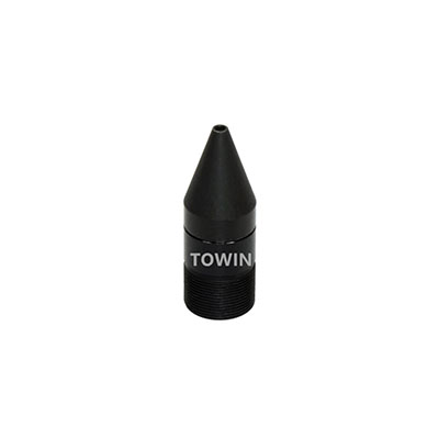
Fixed focus M12 Mount pinhole lens
The Future of Pinhole Lens Manufacturing: Trends to Watch
As industries continue to demand smaller, more efficient optical components, Pinhole Lens Manufacturing is poised for transformative growth. Key trends include:
- Nanoscale Fabrication: Techniques like focused ion beam (FIB) milling are enabling pinholes below 100 nanometers, opening doors to quantum optics and nanophotonics.
- Additive Manufacturing: 3D printing is being explored for creating complex pinhole arrays with embedded functionalities, such as filters or diffraction gratings.
- AI-Driven Optimization: Machine learning algorithms are being used to predict and correct manufacturing defects, reducing waste and improving yield rates.
Conclusion
The evolution of Pinhole Lens Manufacturing is a testament to human ingenuity. From rudimentary drills to laser beams and ion guns, each advancement has pushed the boundaries of what’s possible, enabling applications that were once confined to science fiction. As technologies like EUV lithography and hybrid fabrication gain traction, the future of pinhole lenses looks brighter—and smaller—than ever.